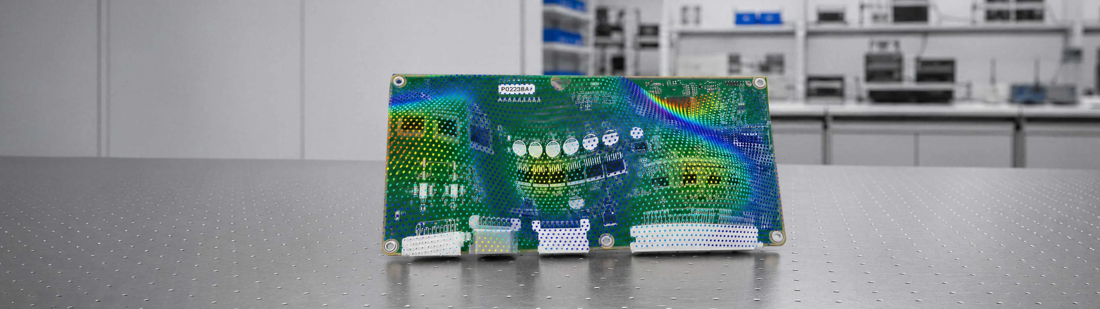
Application report
Vibration Measurement of a Printed Circuit Board (PCB)
How is mechanical stress distributed across a printed circuit board—and which components are affected? Laser Doppler vibrometry provides the spatial response. This report presents three measurement approaches for printed circuit boards (PCBs):
From full-field out-of-plane measurement and 3D vibration analysis to 3D single-point measurement.
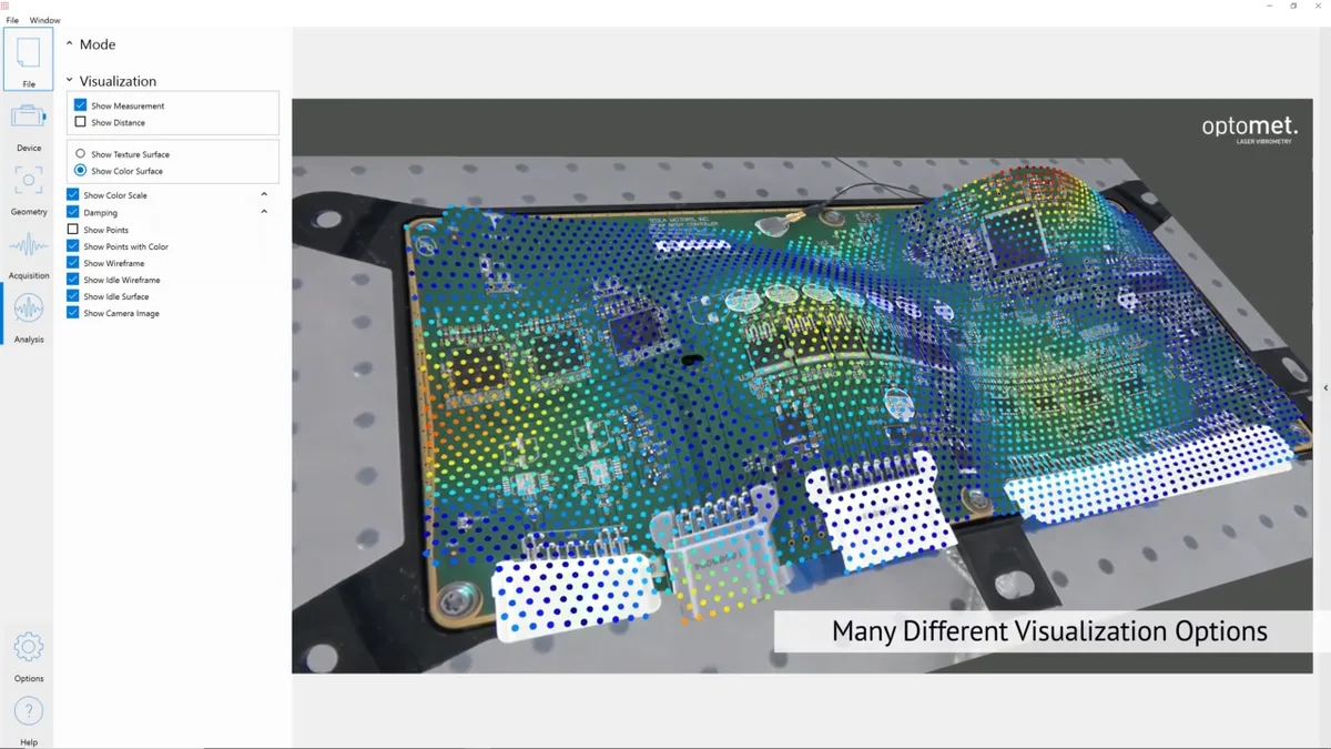
Full-Field Measurement Perpendicular to the Surface (Full-Field, Out-of-Plane)
A vibrometer scans the entire PCB and reveals vibration hotspots at component level.
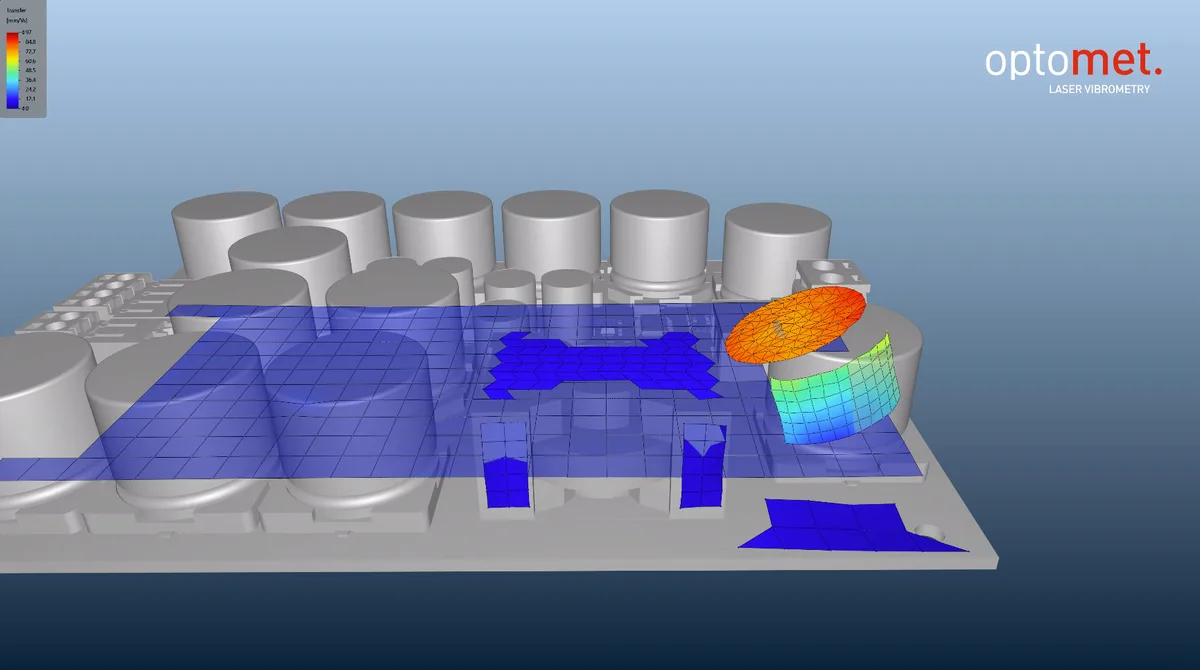
Three-Dimensional Full-Field Measurement (X/Y/Z, In-Plane + Out-of-Plane)
Three synchronized vibrometers capture in-plane motion, tilting motion, and thermal expansion.
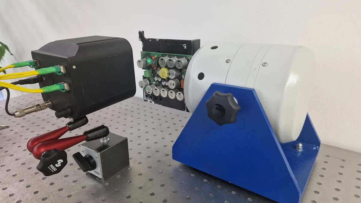
Three-Dimensional Measurement at a Fixed Measurement Point (Single-Point, X/Y/Z, In-Plane + Out-of-Plane)
Compact Fiber Head for 3D measurement at a defined point—ideal for shaker tests.
Full-Field Out-of-Plane Measurement with a Scanning Vibrometer
- Test Specimen
- Populated Printed Circuit Board (PCB)
- Measurement system
- Optomet laser scanning vibrometer
- Software
- SMART Lab
- Analysis
- Full-field ODS, component-level mode shapes
Objective
The aim of this measurement is to visualize the full-field out-of-plane vibration behavior of a populated automotive PCB under controlled excitation. Instead of measuring a single point, the entire PCB surface is scanned to identify where the vibration amplitudes perpendicular to the surface are greatest—at both board and component level. The resulting operating deflection shapes (ODS) reveal which areas and components are exposed to the highest dynamic loads.
1 Measurement setup
The PCB is mounted on an electrodynamic shaker. The scanning vibrometer is installed on a portable aluminum-profile frame above the test specimen, with a perpendicular view of the PCB surface. This configuration provides the optimal measurement angle for out-of-plane vibration measurements.
Measurement setup: Optomet scanning vibrometer mounted on a portable gantry frame, positioned vertically above the populated printed circuit board on an electrodynamic shaker. The compact all-in-one design requires no external DAQ hardware.
The Optomet scanning vibrometer combines a vibrometer, data acquisition, signal generator, and camera in a single instrument. No additional external hardware is required for this measurement. The excitation signal for the shaker is generated directly by the integrated signal generator.
2 Define measurement points in SMART Lab
The SMART Lab software displays a live image of the test specimen via the integrated camera. The measurement area and scan grid are defined directly on this camera image. Area selection tools, mesh generators, and component-based assignment enable precise placement of measurement points—from a coarse full-board grid to dense grids on individual components.
Both images show the component side of the PCB from slightly different perspectives. The measurement areas and boundary tools are defined in the image on the left, while the image on the right shows the completed measurement-point grid. SMART Lab supports multiple layers, allowing different measurement areas—such as a coarse full-board grid and dense grids on individual components—to be managed within a single project.
3 Configure measurement parameters
The vibrometer settings are configured in the Acquisition module. For this PCB measurement, the upper cutoff frequency is 100 kHz—sufficient to capture both the board's fundamental resonances (typically below 5 kHz) and higher-frequency component modes. With more than 13 million FFT lines and a frequency resolution of 6.4 mHz, even closely spaced modes are clearly resolved.
Measurement settings in SMART Lab: 100 kHz maximum frequency, 216 kS/s sampling rate, 10 averages per point. Autofocus and vibration measurement are enabled for the scan.
4 Automatic scanning
Once the scan grid and settings have been defined, the vibrometer automatically scans all predefined measurement points. The laser moves from point to point, readjusts the focus as needed, records the vibration signal, and proceeds to the next position. No manual intervention is required during the scan.
Automated scan in action: The laser independently scans the predefined measurement grid. The green laser spot is visible on the surface of the printed circuit board.
The measurement is entirely non-contact. No sensors on the PCB, no cables, and no additional mass on the structure. The results reflect the assembly's actual vibration behavior.
5 Visualization and analysis
Once the scan is complete, SMART Lab offers various visualization options in the Analysis tab. The vibration data can be displayed as color-coded points overlaid on the camera image, as an interpolated color map, or as a wireframe model with animated deformation. Damping information can also be incorporated into the visualization.
The color-map visualization makes the global plate modes immediately apparent: In this case, a higher-order mode shape is visible, with several pronounced amplitude maxima distributed across the PCB. The location of these maxima relative to the component positions is directly relevant to reliability assessment—components near a vibration maximum experience the highest dynamic loads.
6 Detailed component analysis and video export
In addition to the overall view, SMART Lab lets users zoom in on individual components to visualize their local mode shapes. The integrated video recording feature produces 4K videos of the animated vibration data—including tracking shots that move the virtual camera across the PCB surface. Ideal for presentations and reports.
Detailed component view with video export: Each capacitor displays its individual vibration pattern. The tracking shot function creates smooth camera movements across the circuit board for 4K video recordings.
The detailed view shows how each individual component responds to the excitation. In this close-up, each electrolytic capacitor exhibits its own vibration pattern—some tilt laterally, while others show vertical displacement. This level of detail is only possible with the spatial resolution of a scanning vibrometer and remains undetected by conventional accelerometer measurements.
3D vibration analysis (SMART 3D-Scan)
Real measurement data, not a simulation – The visualization shows an actual 3D vibration measurement of the populated PCB, acquired using SMART 3D-Scan. The measurement data can be projected directly onto the PCB's 3D model, making it immediately apparent which components and areas are affected.
- Test specimen
- Populated automotive PCB
- Measurement system
- SMART 3D-Scan (3 × SMART Scan+)
- Measured quantities
- Velocity in X, Y, and Z at each measurement point
- Visualization
- 3D model mapping, camera overlay, animated mode shapes
Three synchronized SMART Scan+ vibrometers measure simultaneously from different angles.
From the three velocity components, the software calculates the complete motion in the X, Y, and Z directions at each measurement point. The measurement workflow in SMART Lab is essentially the same as for 1D measurements: define measurement points on the 3D model or camera image, scan them automatically, and visualize the results. The key difference lies not in the workflow, but in what the results reveal.
Thermal expansion: the same system, a different application
In addition to vibration analysis, the same SMART 3D-Scan vibrometer can also measure the thermal expansion of the PCB and its components. Differences in the coefficients of thermal expansion of the FR4 substrate, copper traces, solder joints, and housing materials cause localized deformation as temperatures change, potentially resulting in fatigue damage.
For temperature cycling tests (TCT) and thermomechanical reliability assessments, 3D measurement of thermal expansion provides spatial evidence that strain gauges could only capture at a few locations—all without contact and across the entire surface.
3D single-point measurement with SMART 3D-Fiber
- Test object
- ECU (electronic control unit) on an electrodynamic shaker
- Measurement system
- SMART 3D-Fiber (3D single-point vibrometer)
Not every PCB analysis requires a full-field scan grid. For shaker testing of electronic control units (ECUs), qualification of individual assemblies, or monitoring defined measurement points in production testing, a single measurement point is sufficient—provided all three spatial directions are captured.
SMART 3D-Fiber does exactly that: three laser beams converge on the same point on the surface to capture the complete 3D vibrational motion. The compact Fiber Head is particularly well suited to confined installation spaces—for example, when measuring directly on a PCB inside an enclosure.
The X, Y, and Z velocity components are available directly via the digital and analog outputs. SMART 3D-Fiber can be operated either through SMART Lab or directly via an external DAQ system—no proprietary software is required for integration into existing test benches.
Which system is right for which measurement task?
All three measurement approaches presented in this report use Optomet laser Doppler vibrometry and SMART Lab software. The choice of system depends on the information required:
| Scanning vibrometer1D, full-field | SMART 3D-Scan3D, full-field | SMART 3D-Fiber3D, single-point | |
|---|---|---|---|
| Out-of-plane vibration | ✓ | ✓ | ✓ |
| In-plane vibration | – | ✓ | ✓ |
| Full-field ODS / mode shapes | ✓ | ✓ | – |
| Thermal expansion | – | ✓ | ✓ |
Scanning vibrometer for PCB vibration analysis
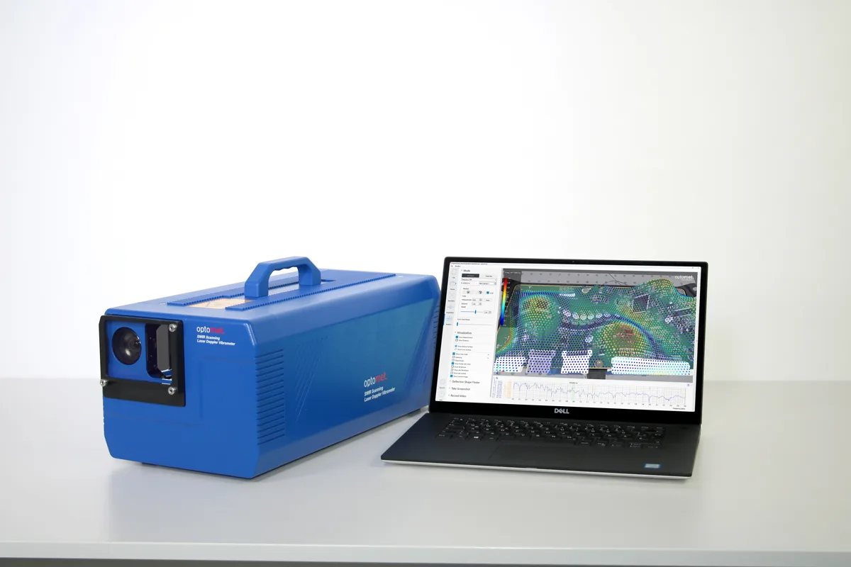
CLASSIC Scan
Scanning laser Doppler vibrometer with SWIR technology (1550 nm), eye-safe measurement laser (Class 1), and digital FPGA signal processing.
- Frequency bandwidth: DC to 10 MHz (24 MHz)
- Max. velocity: 25 m/s
- Grid density: up to 512 × 512 points
- Weight: 12 kg
- Full HD camera, 30× optical zoom
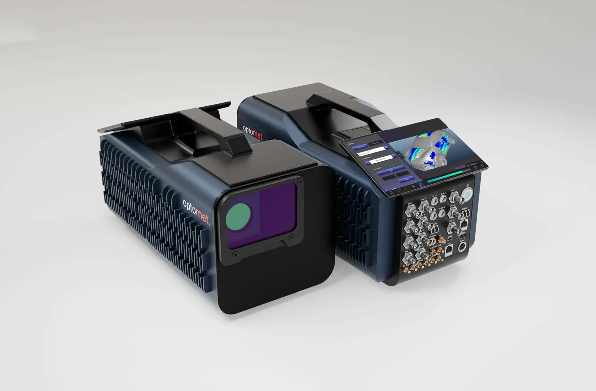
SMART Scan+
The latest generation: a fully integrated scanning vibrometer with extended bandwidth, 4K camera, integrated DAQ, and up to 12 reference channels – no external hardware required.
- Frequency bandwidth: DC to 50 MHz
- Max. velocity: 50 m/s
- Grid density: up to 512 × 512 points
- Weight: 8.2 kg
- 4K camera, 20× optical / 40× hybrid zoom
- Integrated DAQ & signal generator
- Up to 12 reference channels (IEPE/TEDS)
- Wi-Fi 7, Bluetooth 5.2, GNSS
- 7" Touchscreen, SMART Lab Software
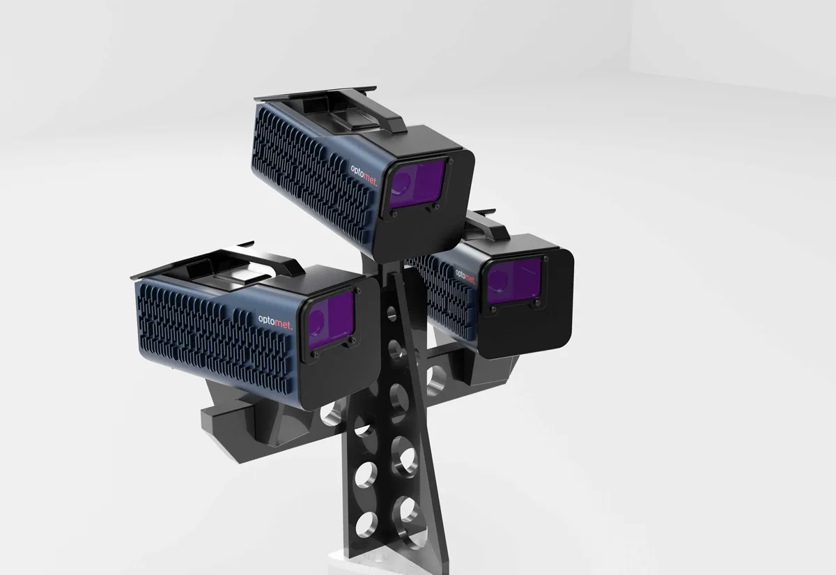
SMART 3D-Scan
Three synchronized SMART Scan+ units for complete X/Y/Z measurements at every scan point. Modular upgrade path.
- 3 × SMART Scan+
- Synchronized 3D acquisition
- Each unit can also be used independently
- Up to 36 reference channels
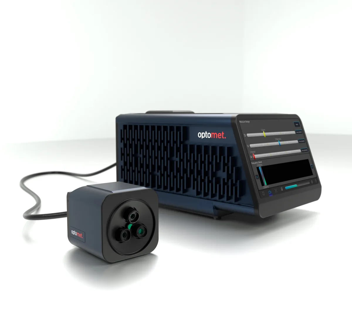
SMART 3D-Fiber
3D single-point vibrometer with compact Fiber Head. Direct X/Y/Z output via analog and digital outputs.
- Compact 3D Fiber Head (107 × 100 × 102 mm)
- Working distance 83 mm
- Integrated webcam for alignment
- Operation via SMART Lab or external DAQ
The basic measurement process is similar for all four systems. The choice depends on the measurement task: full-field or point-based, 1D or 3D—or both, as the SMART systems can be combined and expanded incrementally.
Summary
This application report presents three approaches to vibration analysis of populated printed circuit boards using Optomet laser Doppler vibrometers.
Full-field out-of-plane measurement: A single scanning vibrometer captures the vibration component perpendicular to the PCB surface. Six steps, from setup to detailed component analysis, demonstrate the complete workflow. The results identify spatial vibration hotspots, visualize mode shapes at PCB level, and reveal the individual vibration behavior of specific components.
3D vibration analysis: Three synchronized SMART Scan+ vibrometers capture the complete motion in X, Y, and Z. This reveals lateral motion, tilting motion, and coupled modes that remain hidden in out-of-plane measurements. The same system also captures thermal expansion—relevant to assessing thermomechanical reliability.
3D single-point measurement: The SMART 3D-Fiber provides complete 3D vibration data at a defined measurement point. The compact Fiber Head is ideal for shaker testing of electronic control units, component qualification, and integration into existing test rigs.
All three approaches provide spatial evidence for informed design decisions: component relocation, local reinforcement, adjustment of mounting conditions, or FEM validation against measured real-world data.

Looking for full-field vibration analysis of your PCBs? Optomet offers the right measurement solution.
Contact